
Nanofibers for Memristive Neural Networks
In the fields of neuroscience and artificial intelligence, there is a strong need for a large-scale model of the brain. Such a model would not only enable a greater functional understanding of the human brain and its ailments, but also open new doors in data analysis, further understanding of human and machine learning processes, and the overall behavior of dynamical systems. Compared to biological brains, current artificial neural systems are much less efficient in terms of power consumption, connectivity, and neural density. Moreover, with Moore’s law approaching the end of its applicability lifetime, it is clear that a radically new approach to neural hardware is required if we want to emulate the power and efficiency of the brain. To this end, we have recently developed a novel method for connecting silicon neurons that models the plasticity and connectivity of brains, eliminates the need for complex architectures, and functions with both digital and analog neural circuits.
Rather than hardwiring connections onto the neural circuit itself, which is extremely space intensive for large, highly connected networks, the neurons are interfaced with a nonwoven mat of conductive nanofibers. These nanofibers have a coaxial structure: a conductive core to transmit signals between neurons, and a shell made of a memristive material, which insulates individual fibers from one another and also allows for the formation of modifiable synapses at each neuron. The input and output electrodes (or biologically, the dendrites and axons) of each neuron on the chip make direct electrical contact with a large number of nanofibers, and the voltage on these electrodes causes current to flow through the memristive shell and into the core of the fibers. This current is then transmitted to neurons connected to the same fibers. The memristive junction between the fiber core and electrode creates a synapse whose weight can be adjusted via spike-timing-dependent plasticity, the same learning rule used by biological neurons.
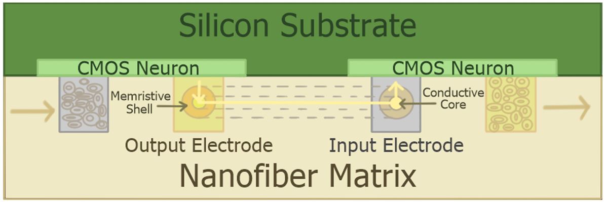
Schematic of the architecture derived from electrospun fibers
Electroceramic Nanofibers
In the last decade, several research groups have been working in the use of electrospinning for production of ceramic fibers. Electrospinning is a continuous process allowing for the production of nanofibers relatively easily with the versatility to adjust fiber morphology and produce different ceramic systems. Ceramic nanofibers are attractive because of their high surface area to weight ratio, long length and high porosity, allowing for a wide array of potential applications. Some of the potential applications include air and water filtration, gas sensors, superconductor membranes for gas separation, nanoelectronics, nanofluidic applications, tissue engineering scaffolds, optical devices, energy conversion and photocatalysis. The ceramic systems that we are currently working on are TiO2, Bi2Sr2CaCu2O8+x, Bi2Sr2Ca2Cu3O10+x, YBa2Cu3O7-d. The goal is to adjust the thermal cycle to grow large crystals in the structure through homogeneous nucleation. Single crystal ceramic fibers can lead to improved properties.
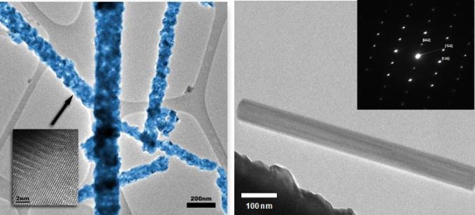
TEM images showing BaTiO3 electroceramic nanofibers
Since its discovery, the Bi2Sr2Can-1CunO2n+4+x (BSCCO) family has been the focus of intense interest with several methods existing for the synthesis of BSCCO. While reducing the diameter of superconducting wires is highly desirable, there is concern, however, regarding the critical size limit in which superconductivity can be sustained. This work focuses on the synthesis and characterization of Bi2Sr2CaCu2O8+x superconducting nanowires. The electrospinning process is a relatively simple, inexpensive, and scalable bottom-up approach for obtaining materials with nanometer features. Bi2Sr2CaCu2O8+x nanowires with a Tc = 78.7 K are synthesized using the electrospinning process employing sol-gel precursors. A sol-gel methodology is used to obtain a homogenous PVP solution containing Bi, Sr, Ca, and Cu acetates. Mats of randomly oriented nanowires and aligned nanowires are also collected. After a heattreatment at 850 °C in ambient atmosphere using heating rates of 100 and 400 °C/h, fully crystallized Bi2Sr2CaCu2O8+x nanowires are obtained. The morphology, microstructure, and crystal structure of these nanowires are then examined to reveal a rectangular morphology having typical wire thickness in the range of 150 to 250 nm, and a wire width between 400 to 600 nm. DC magnetization studies are conducted to investigate the critical transition temperature (Tc) of Bi2Sr2CaCu2O8+xnanowires and to compare their magnetic properties to those of bulk Bi2Sr2CaCu2O8+x powder. The Tc for the commercial powderis observed at 78.6 K, and that of the obtained nanowires at 78.7 K. These results point to the superconductivity nature of Bi2Sr2CaCu2O8+x nanowires, and the potential of the electrospinning process for the synthesis of this superconductor material.
Chitosan Fibers
Chitosan is derived from chitin which is the second most abundant natural polymer. Our research plan is to create water filtration systems made of chitosan fibers over a range of diameters and test their ability to adsorb heavy metals, specifically mercury ions. Extrusion, Heat-aided Jet Spinning and Electrospinning are the processes primarily used for producing chitosan fibers of varying diameters. Filters are made by encasing the fibers in a rigid, structural support. Cold-Vapor Atomic Fluorescence Spectrometry (CVAFS) is used to measure the mercury levels in water before and after filtering.
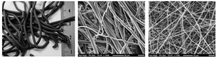
Chitosan macrofibers, microfibers and nanofibers (from left to right)