
Ionic Conductors
Solid oxide fuel cells (SOFCs) have received increased attention in recent years as an environmentally friendly power source, particularly those which operate in the intermediate temperature (IT) range of 400 – 800°C. This is due to their flexibility in design, wider range of useable fuels, and potential uses in distributed and portable power. However, current SOFCs do not provide sufficient power at these intermediate temperatures and must operate at or above 1000°C which is far too high for use in technologies such as fuel cell vehicles (FCVs). A key component of an efficient IT-SOFC is a solid oxide electrolyte with a high ionic conductivity at intermediate temperatures. Our group continues to investigate the properties of rare earth doped ceria, the most promising material for use in IT-SOFC electrolytes.
Current work involves the synthesis and characterization of doped ceria thin films deposited using both pulsed laser deposition (PLD) and chemical solution deposition (CSD). Ionically conducting thin films not only have applications in micro-SOFCs, but also allow for the direct measurement of material properties such as grain ionic conductivity, by measuring films of varying microstructure.
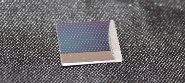
Epitaxial doped ceria thin film on a platinum bottom electrode using PLD
It is well known that grain boundaries can be detrimental to conduction. To characterize the blocking nature of grain boundaries, our group is working on lamellae cut from 10 mol% doped ceria pellets with average grain sizes greater than 10 micrometers using focused ion beam techniques. The lamellae are fashioned into structures mimicking the dimensions of thin film electrodes and tested using impedance spectroscopy to determine the electrical response through a single grain, a grain boundary (of varying orientation to the direction of ionic conduction), and a triple point. This can elucidate the effects of not only grain boundaries but strain, electrode interfaces, and other extended defects as well.
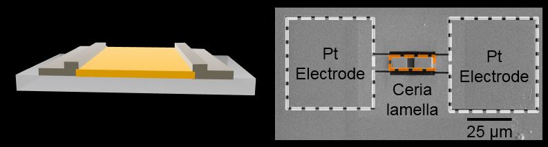
Single grain lamella
Tunable Dielectrics
The objective is to design, characterize and model a new class of bismuth based tunable metamaterials for high power, low loss, RF applications. The proposed applications include an ultra-compact, highly linear, high power handling, tunable waveguide filter in low GHz operation. When an air-filled rectangular waveguide has a dimension of xyz , it has a cutoff frequency with a corresponding wavelength of 2x. Now the space is filled with two materials: (1) a dielectric material with a dielectric constant of εr and its breakdown voltage higher than that of air by k1 times, and (2) a tunable slab with an SRR (split ring resonator) array on a thin film tunable layer constructed in the middle of the waveguide, where the resonance frequency fr of SRR is k2 times smaller than that of the cut-off frequency of the original waveguide. The resultant waveguide showing an equivalent frequency response is dimensioned as (x/(k2√εr))(y/k1)(z/√εr) for TE10 mode operation. The passband is tuned by applying a bias voltage on the slab. The loss tangents of the filling dielectric material and the SRR slab, and the conductor loss of SRRs are designed to be small with low GHz operation. If the filling dielectric material has a dielectric constant εr of 20 and a breakdown voltage factor k1 of 100, and the SRR frequency factor k2 of 5, an overall scaling factor of 104 is achieved.
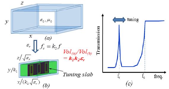
Waveguide filter scaling: waveguide with (a) air dielectric and (b) εr dielectric and an SRR tuning slab; (c) frequency response.
Bandgap Tailoring
The goal of this project is to produce a thin film whose electronic properties vary through its thickness. Complex oxides with strong corrected electrons usually possess novel properties like tunable band gap, abrupt metal-insulator transition (MIT), etc., which can be triggered by chemical composition, or thermal, electrical, optical perturbations. If the required external excitation is small enough, we could then probably build tunable electronic devices. The Vanadium dioxide (VO2) is a good example, as possessing thermally triggered MIT at ~ 340K, which is very close to room temperature. This is associated with the abrupt phase transition from a monoclinic insulator to rutile metal at a very narrow temperature range. VO2 was then found to have electrically triggered MIT as well, which is very intriguing, as metallic and insulating states are reversible or tunable in this material. Therefore these types of correlated materials with metal-insulator transition is worth investigating as promising candidates for channel materials due to its ultrafast phase transition property.
In this project we investigate pyrochlore molybdates (A2Mo2O7), studying its electron-correlation induced metal-insulator transition, and tunable band gap by optical spectroscopy. A2Mo2O7 undergoes a magnetic phase transition from the spin-glass insulating state to the ferromagnetic metallic state. The transition point seems to fall on A = Gd, i.e. Gd2Mo2O7, which is located at the barely insulating side of the phase diagram with almost zero gap. In this work, we study Gd2Mo2O7 (GMO) as the base material, to investigate the solid solution between a correlated metal GMO and a band insulator Gd2Ti2O7 (GTO). This B-site substitution would offer a very interesting system i.e. Gd2(Mo1-xTix)2O7, to study its composition dependent metal-insulator transition or tunable band gap behaviors. Current research focuses on refining thin film techniques and defining the structure-properties relationship in the chosen pyrochlore system.